Development of Light Absorber-Catalyst Artificial Photosynthesis Assembles
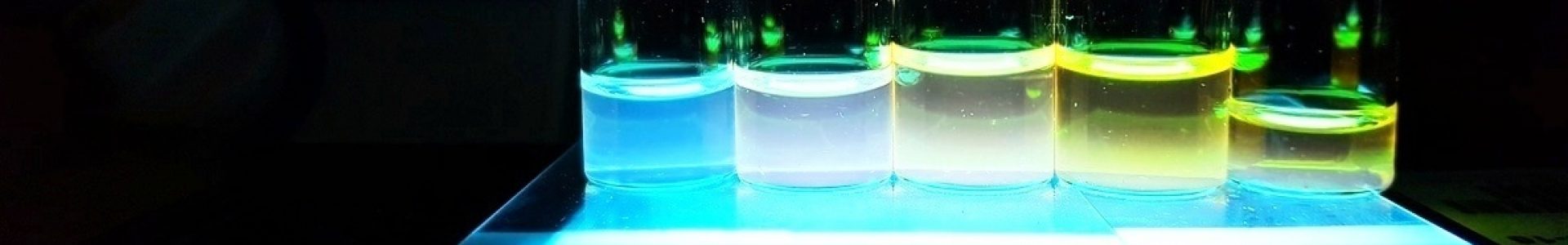
Semiconductor electrodes that have been modified by molecular catalysts have been investigated extensively with various polymeric backbone attachments. However, few studies have been focused on the direct attachment of molecular catalysts onto semiconductor surfaces. By carefully adjusting the energetics between semiconductor and molecular catalyst interface, the efficiency of energy extraction from the photogenerated electron-hole pairs can be optimized. Adding an active catalyst unit to the surface of semiconductor is a feasible strategy to both improve the stability and maintain catalytic activity of a photoelectrochemical device. In a previous study we showed that by using an atomic layer deposited TiO2 layer as well as an earth abundant molecular catalyst we were able to protect the GaInP2 surface.
Understanding the Electron and Energy Transfer Mechanism in Light Harvesting Systems
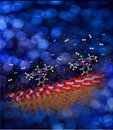
In the natural photosynthetic process, chemical energy is generated by light conversion followed by proton and electron transfer events (or proton coupled electron process). This process typically begins with light being absorbed by a harvesting pigment. The energy generated by light absorption is then transferred through different chromophores via energy cascade and eventually reaches a reaction center. At the reaction center, the light energy is converted to chemical energy through a multi-electron, multi proton transfer reactions. The basis of artificial photosynthesis is to mimic the photosynthetic process using semiconductors and molecular catalyst assemblies. Through an improved understanding of the coupled electron and energy transfer process in design assemblies could provide significant information for the future design and implementation of industrial scale artificial photosynthesis systems.
Using Bio-Photo Hybrid Systems for Efficient Fuel Generation
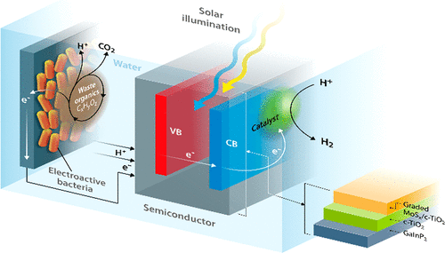
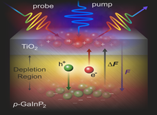
To drive a complete water splitting reaction the semiconductor material must absorb irradiation with photon energies larger than 1.23 eV. In other words, the band gap energy of semiconductor should be larger than 1.23 eV. Accounting for concentration and kinetic overpotential losses, the practical absorption energy needed for driving water splitting ranged from 1.6-2.3 eV. If the band gaps of semiconductor are lower than this range, water splitting will require an external electrical bias to occur. Such requirement of bias complicates reactor systems, reduces energy outputs, and increases the cost of artificial photosynthesis. In the meantime, in order for the photoinduced free carriers to travel to the semiconductor-liquid junction and react with water, the conduction band and valence band positions of the semiconductor must straddle the water reduction and water oxidation potentials. As a result, there are only few semiconductor materials that could meet this requirement, such as Cu2O and TiO2. In our future research, we are interested to found out alternative bio and photo combined method for lowering the overall thermodynamics for the fuel generation.